An Investigation of Non-Ideal Op Amp Characteristics
Greg Westfall
Date: 11/22/2023
Introduction
In this lab we investigated the non-ideal characteristics of an op-amp. Unlike many other labs, the LM741C IC was used for it’s lackluster non-ideal performance. The LM741C is an older chip which performs much worse than newer op-amp IC’s. For this lab we investigated the input DC parameters of the op-amp (door 1). We measured the offset voltage Vos, the input bias currents IB, and the offset current Ioss. Three different configurations of a circuit were used to measure these parameters.
Circuit Design and Reasoning
Input Offset Voltage
The circuit below was used to measure the input offset voltage of the op-amp. By tying all inputs to ground, the only source for the op-amp is the offset voltage. The circuit below was used to measure the offset voltage.
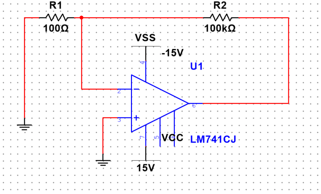
Figure 1: Circuit for Measuring Offset Voltage
With the inputs tied to ground, the only source influencing the output voltage is the input offset voltage. The op-amp was configured as an inverting amplifier, with a gain of 1001 = (R2/R1 + 1). By measuring the output voltage we can easily gather the input voltage by using the relationship Vin = Vos = Vout/1001.
Input Bias Currents
Two different circuits were used to obtain the input bias currents IB1 and IB2 for the op-amp. The first circuit used is given below.

Figure 2: Diagram for Circuit to measure IB1
Before taking measurements, Vos was removed by using the offset null pins of the op-amp. This is not shown on the diagram to remove complexity. With the contribution of Vos to the input being zero, we are left with the bias currents. Since Vos = 0, V+ = V– = 0. And so we can measure IB1 by measuring the voltage across R3 and applying Ohm’s law.
The circuit for measuring IB2 is similar and is given below.

Figure 3: Diagram for Circuit to Measure IB2
The voltage at the positive terminal is given by IB2*R4. This is the only source of input to the op-amp, and so we can measure the output voltage, and use Ohm’s law as with IB1 to find IB2.
Input Offset Current
The input offset current is given by 𝐼𝑜 = |IB1 − 𝐼𝐵2|. We use the measurements above to find Ios.
Data and Discussion
Input Offset Voltage
The input offset voltage was measured to be 0.7mV. The typical value of the input offset voltage is around 1mV according to the datasheet. The input offset voltage was also simulated.

Figure 4: Simulation of Input Offset Voltage
Since the input offset voltage is given by Vos = Vout/1001, we have Vos = 1mV.
The simulated value of Vos and the value from the datasheet are effectively the same. The measured value of the offset voltage is 30% lower than the typical value, which is good since an op-amp would ideally have as low an offset voltage as possible.
One potential source of error is the gain of the op amp being slightly different than expected due to inexact resistor values. In the future the resistor vales will be measured for more exact calculations.
Input Bias Currents
The measured input bias current was 50nA for IB1 and 52.3nA for IB2. This averages to an IB of 51.1nA. The typical value of the input bias current is 80nA according to the datasheet. The input bias current was determined in simulation as well.
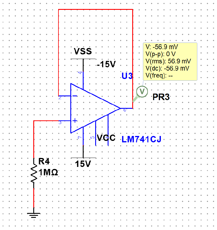
Figure 5: Simulation of Input Bias Current 1
An attempt was made to use the offset null pins in simulation to reduce the offset voltage before measuring the offset current, however these pins seem to have no affect on the output in simulation despite having positive results experimentally. IB1 was measured to be 56.9nA.
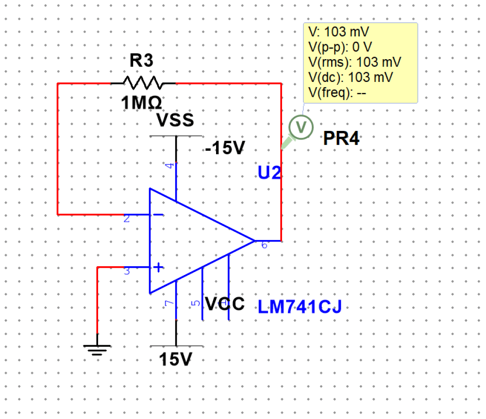
Figure 6: Simulation of Input Bias Current 2
IB2 was measured to be 103nA in simulation. This averages to an IBsim of 80nA. The simulated value of IB and the value from the datasheet are the same, which is similar to what was obtained for the offset voltage. The experimental bias current was 38% lower than the typical bias current from the datasheet. Again, this is good since ideally the bias current would be 0. Sources of error were minimalized by removing the offset voltage from the output. One potential source of error is the resistance of the 1MΩ resistor being slightly different than advertised, however this wouldn’t change the bias current measurement very much.
Input Offset Current
The input offset current was obtained from the measurements of IB1 and IB2 and is 2.3nA. The typical value of this offset current is 20nA according to the datasheet. The value obtained in the simulation was 46.1nA. The experimental input offset current was much lower than the typical value and far below the simulated value. It is 88.5% less than the typical value. The sources of error for the input offset current are the same as above.
Summary and Conclusion
Effects of Input DC Parameters
The input DC parameters have a relatively large effect on the output of an op-amp when working with smaller signals, however this effect is diminished when the signals become larger. When input signals are small the effect of these parameters should be considered. As shown in the experiments, at a gain of 1000, the input offset voltage contributes 1V to the output, which is negligible.
Comparison of the 741 Op-Amp to Others Available
According to a quick internet search, one of the best available op-amps is the OPA310 from Texas Instruments. The OPA310 has an input offset voltage of 0.25mV, an input bias current of 1pA, and an input offset current of 0.5pA. This means that the input offset voltage of the 741 is 60x more than the 310, the input bias current is 80,000x more than the 310, and the offset current is 40,000x more than the 310 when comparing each of their typical parameters from the datasheets.
