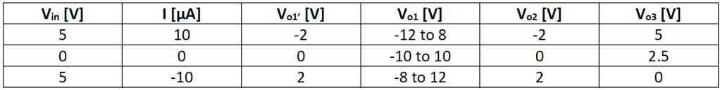
Design of a Rocket Probe Signal Conditioning Circuit
Greg Westfall
Date: 11/19/2023
Introduction
This report outlines the creation of a Rocket Probe Signal Conditioning Circuit. The circuit measures the current of charge collected by a rocket probe, converting that current to voltage, removing unwanted common-mode signals, and finally processing the signal to ensure compatibility with the telemetry system. A design based on op-amps was decided due to the ease of cascading op-amps with other op-amps to achieve a desired outcome. The requirements for the circuit are defined below.
An overall final schematic for the circuit is provided below.
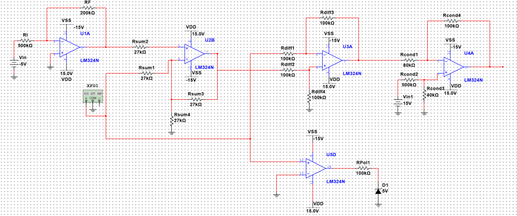
Circuit Design and Analysis
Current to Voltage Amplifier
The first step in the circuit attenuates and inverts the input signal following the requirements in Table 1. Vo1 is the output of this stage of the circuit. The final schematic for this portion of the circuit is provided below. The circuit takes in the small current (represented by a voltage source and a 500kΩ resistor) and converts this current to a voltage for future processing. The first amplifier provides a -2V output if the input current is 10μA, a 0 V output for 0 input current, and a 2V output for a -10μA input. The second op amp combines this output with a separate 20Vpp signal for biasing.
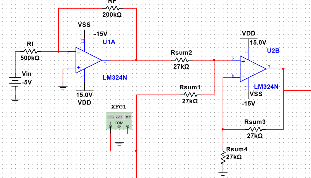
The requirements specified that the output of the first op-amp be an inverted and attenuated version of the input. The relationship is given by 𝑉𝑜1′=−2/5*𝑉in . This gives a gain of -2/5 V/V. The gain of an inverting amplifier is given by AV=−RF/RI
Thus, the ratio of RF to RI should be 2 to 5. And so choosing a 500kΩ resistor for RI implies that RF should be 200kΩ.
Moving to the next op-amp, we would like to combine (or sum) the output of the first op amp with a 20Vpp signal. A simple summing amplifier is used for this purpose. The output of a summing amplifier is given by 𝑉out=[1+ R𝑠um3/R𝑠um4]Vin
Where Vin is the average value of the two inputs. And so keeping Rsum3 = Rsum4 = 27kΩ provides the expected output.
Difference Amplifier
The difference amplifier section of the circuit removes the 20Vpp bias signal from the original signal by using a difference amplifier.

Th input of the V– terminal of the op amp is the 20Vpp sine wave while the input to the V+ terminal is Vo1. The output of a difference amplifier is given by Vout = Rdiff3/Rdiff1(V+ – V–) when Rdiff1 = Rdiff2 and Rdiff3 = Rdiff4. Thus, setting all resistors equal gives us the required output of Vout = V+ – V– = Vo2.
Signal Conditioner
The signal conditioner converts the output of the difference amplifier to something a signal that the telemetry system accepts.
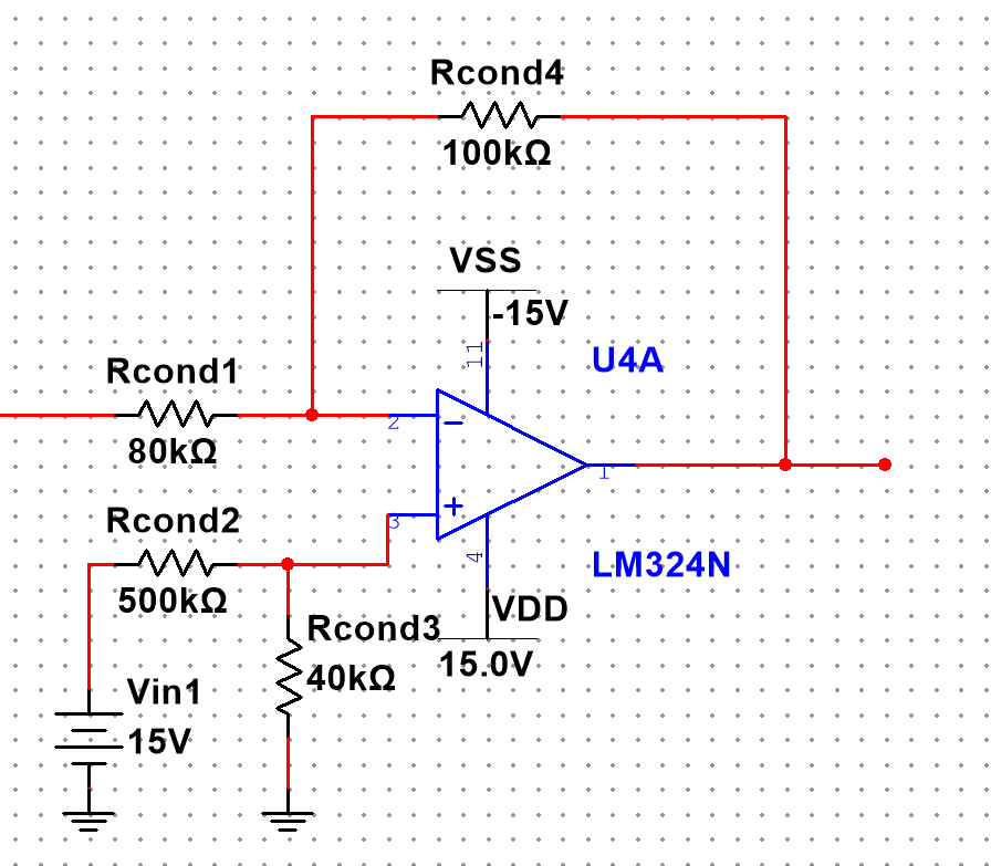
The telemetry system only accepts signals in the range of 0 to 5V, with 2.5V being the middle range. To do this a version of a difference amplifier is used with the positive input of the op-amp kept at a constant voltage. The general relationship for this type of configuration is given by Vout=A*Vin+B where A= (Vout;1− Vout;2) / (Vin;1−Vin;2) and B is the offset when Vin is equal to 0.
When Vin = Vo2 = 0, Vo3 = Vout is expected to be 2.5V. Hence B is 2.5V. A can be determined by using two points from the requirements.
To determine the resistor values, we use the relationships B= Rcond3/(Rcond3 + Rcond2)(1+ Rcond4/Rcond1) and A = -(Rcond4/Rcond1).
Letting Rcond2= 500kΩ and Rcond1 = 80kΩ along with the values A = -1.25 and B = 2.5 gives us Rcond4 = 100kΩ and Rcond3 = 40kΩ.
Polarity Monitor Subsystem
Since the polarity of the probe voltage is of interest, a polarity monitoring subsystem is used to provide this information. The circuit used is a comparator, which is a nonlinear op-amp circuit.
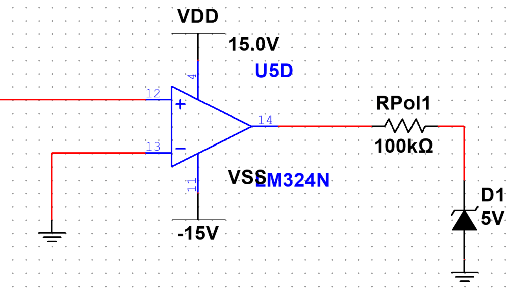
The noninverting terminal of the op-amp is connected to the probe. The op-amp outputs a positive voltage when the input is positive, and a negative voltage when the input is negative. A Zener diode ensures the output is either 5V, for positive input voltages, or 0V for negative input voltages.
Data and Discussion
Experimental Data
The table below outlines the experimental values obtained for the implemented circuit.
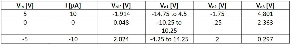
Overall, the results of the circuit are quite good. The polarity monitor works as expected and the output voltage correctly corresponds to the input. The percent error of Vo3 is very low at around 4%, however the error of Vo2 is much higher at around 12%. This is due to improper settings on the measurement from the oscilloscope. Rather gathering the mean output from Vo2, the max and min output were gathered. This provides a relatively inaccurate measurement of Vo2 compared to what is possible, resulting in a larger and unreasonably small percent error for the two measurements above.
Summary and Conclusion
Overall, the rocket probe monitoring circuit design works as expected. All output voltages were quite close to the specifications that were aimed for. Although this was a tedious design, each op-amp stage was relatively straight forward to design and implement. A lot was learned about op-amps, including their different configurations, solving op amp circuits, and their linear/nonlinear properties.
Contact: gregwestfall20@gmail.com
